The WSPR Beacon Project
The multi-band WSPR beacon project has the following objectives:
- To use the smallest available micro controller
- To support 10,15,20,40,and 80 meter bands
- To have a LCD display to show what the WSPR beacon is doing
- To keep Time synced using GPS information
- Runs using a 5v USB charger
High Level Architecture:
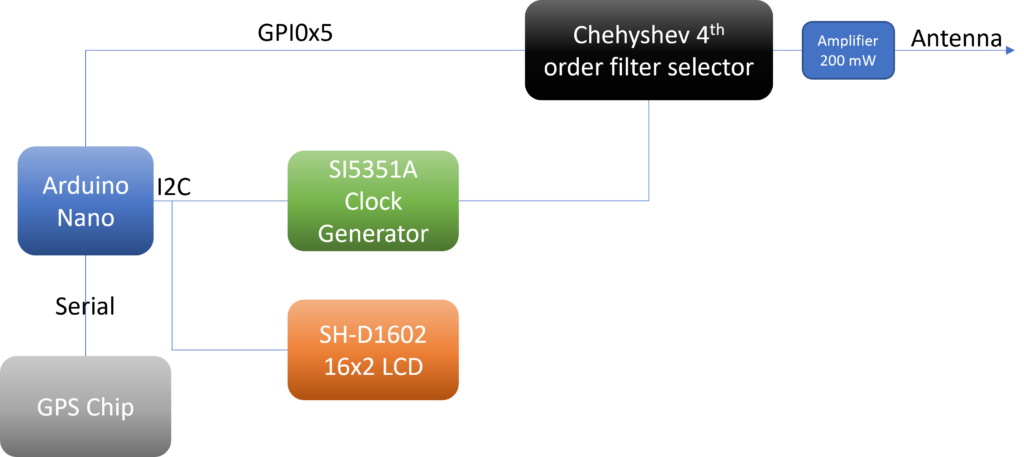
- The Arduino Nano is a small micro controller (32k program flash, 2k of RAM) which is the “brains” of the entire beacon.
- The SI5351A is the primary WSPR signal generator. It generates a square wave at the frequency requested over the I2C bus
- The GPS chip is used exclusively to provide a time reference since the Nano can’t connect to the internet. At some point in the future it may be able to provide the maidenhead grid reference but not in this version.
- The SH-D1602 16×2 LCD will continuously report the call sign, band, and current time
- The Chevyshev4th order filter selector is a I2C controlled filter selector that will insert the right low pass filter for the band being transmitted.
- Finally the amplifier is a broadband RF amplifier that will boost the low power filtered signal.
The 4th Order Chebyshev Filter Selector
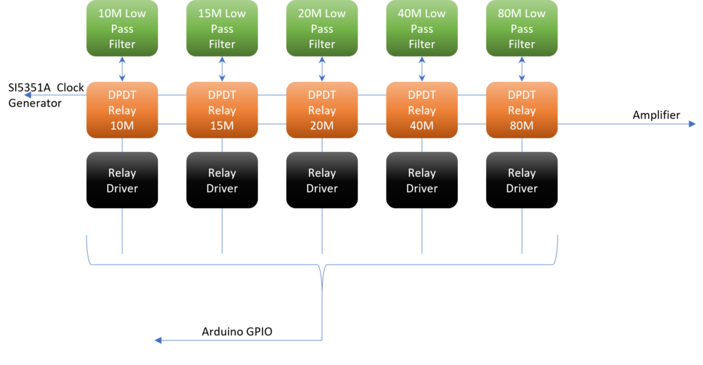
The filter selector is controlled using the I2C bus through a PC8754 8 bit bus extender IC. Each of the filters can be individually switched in or out of the circuit from the SI5351A clock driver and the amplifier. The relay drivers are simple N channel MOSFET (2N7000) driver circuits as shown below.
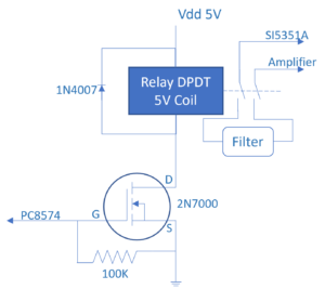
This circuit is designed with readily available parts (amazon). The 100K resistor is not strictly necessary as long as your control line to the gate never floats. If there is a risk of the control line being floated, then add the resistor to avoid any issues. The 1N4007 diode (flyback, flywheel) prevents back EMF from the coil, when the voltage is cut off, from damaging the MOSFET.
The relays are also readily available (amazon). They’re DPDT which enables the start and end of each filter to be switched in or out. A SPDT can also be used by connecting the clock to the input of all filters and using the SPDT relay to switch the appropriate filter into the amplifier. Or conversely connecting all the filter outputs to the amplifier and using the the SPDT relay to switch the clock to the input of each filter. This could cause problems since the filters are shunt/series types where the shunts for lower frequency filters could cause issues for the higher frequencies which is why the DPDT relays are preferred.
The LCD Display
The LCD display will provide a status of the beacon. Currently the plan is to show the call sign, the band, the power, and the current time. The top left where WSPR is shown on the image will be a progress bar on the current transmission.
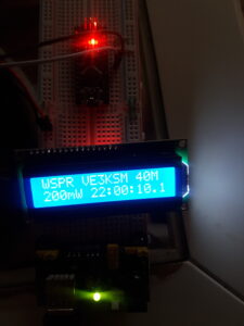
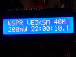
The image shows how this will be laid out on the display which is a small 16 character by 2 row display. The LCD display uses the following ICs:
- HD44780U LCD driver controller
- PCF8574 I2C extender controller
How these two interact will be covered later in the software section.
The GPS chip
The GPS chip is used to get an accurate time reference. With a device that can connect to the internet NTP can be used for this. This minimal implementation doesn’t have the luxury of internet connectivity. The advantage of a GPS chip is that this WSPR beacon can run in the field where no internet connectivity exists. The GPS chip uses the NMEA protocol over the serial port which is very chatty. During a WSPR transmission it would be very difficult to service the serial interrupts without introducing unnecessary jitter in the WSPR protocol transmission. To avoid this the GPS chip is monitored continuously for time updates between WSPR transmissions but once a WSPR transmission begins, an internal clock free-runs until the transmission is completed. Given the master clock for the micro-controller is crystal controlled free-running during transmissions shouldn’t introduce any noticeable error in the transmission. Furthermore, the critical timing of the start of transmission will be closest to the most recent time synchronization with the GPS chip.
The SI5351A clock generator
This clock generator takes commands from the I2C bus and outputs the desired frequency as a square wave. There are 2 clocks available on the clock generator but only one will be used.
The amplifier
The amplifier is a simple broadband amplifier to boost the signal from the filtered clock generator signal to approximately 200mW. The amplifier is based on the readily available 2N7000 N channel FET also referred to as a FETlington because if its darlington type high gain.
The 4th order low pass filters
Currently the design supports 5 bands 10m, 15m 20m, 40m, 80m the WSPR frequencies for these bands are:
| Band | Dial Frequency | Transmit Frequency |
|---|---|---|
| 10m | 28.1246 | 28.126000 – 28.126200 |
| 15m | 21.0946 | 21.096000 – 21.096200 |
| 20m | 14.0956 | 14.097000 – 14.097200 |
| 40m | 07.0386 | 07.040000 – 07.04020 |
| 80m | 03.5926 | 03.594000 – 03.59420 |
All filters are Chebyshev 4th order filters and have the same design. The only difference between the filters are the component values. The cutoff frequency for each filter is set to the upper transmit frequency shown in table 1. There are many on-line filter calculators available to calculate the component values with some using standard values making it much easier to construct the filters. The one I used is here. The graphs that are displayed below were generated by LTSpice which is free circuit simulator software that you can get from analog.com.
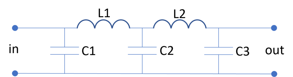
| Band | Cutoff Frequency | C1 | C2 | C3 | L1 | L2 |
| 10 m | 28.1262 MHz | 130 pF | 220 pF | 130 pF | 390 nH | 390 nH |
| 15 m | 21.0962 MHz | 180 pF | 300 pF | 180 pF | 510 nH | 510 nH |
| 20 m | 14.0972 MHz | 270 pF | 430 pF | 270 pF | 750 nH | 750 nH |
| 40 m | 7.0402 MHz | 510 pF | 910 pF | 510 pF | 1.5 uH | 1.5 uH |
| 80 m | 3.5942 MHz | 1.0 nF | 1.8 nF | 1.0 nF | 3.0 uH | 3.0 uH |
The input and output impedance should be matched to ensure the filter operates as expected. The chosen impedance for both input and output is 50Ω. Since the output impedance of the SI5351A is about 85Ω it needs to be match to the expected 50Ω impedance of the load (antenna). A 85Ω to 50Ω difference in impedance isn’t really a big deal and matching is not critical. But to maximize power transfer, the easiest way to do this is to use an L pad matching network:
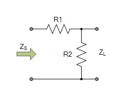
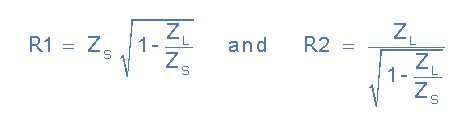
With the formulas above, R1 = 54.5Ω and R2=77.9Ω.
Programming the SI5351A clock generator
The SI5351A clock generator is controlled using the I2C bus.